Interconnection Issues between Memory and Logic in an IRAM System
1. Introduction
 In IRAM systems [1],
the interconnection scheme between
DRAM memory and the processor is a critical system component for many reasons.
Such a scheme has to
meet the processor requirements for high memory bandwidth, low memory
latency and the ability to serve multiple independent data (address)
streams in parallel, in order to achieve high system performance.
In the same time,
it has to be area efficient, in order to reduce cost and increase the area
available for on-chip memory, and have reduced power consumption. An additional
constrain is that the interconnection scheme should not affect the normal
operation of the memory blocks.
In IRAM systems [1],
the interconnection scheme between
DRAM memory and the processor is a critical system component for many reasons.
Such a scheme has to
meet the processor requirements for high memory bandwidth, low memory
latency and the ability to serve multiple independent data (address)
streams in parallel, in order to achieve high system performance.
In the same time,
it has to be area efficient, in order to reduce cost and increase the area
available for on-chip memory, and have reduced power consumption. An additional
constrain is that the interconnection scheme should not affect the normal
operation of the memory blocks.
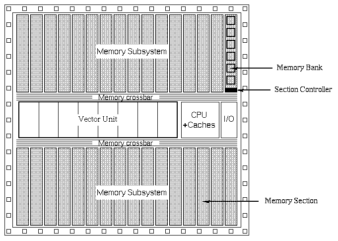
Figure 1. Vector IRAM system floorplan.
The potential floorplan of an
IRAM system using a vector unit as its main processor is presented in figure 1.
Each slice of the vector processor,
called lane, contains one or more load/store units that need to
be interconnected with the memory subsystem. Multiple load/store units would
also exist on-chip if some other processor architecture such as multiscalar,
VLIW or multiprocessor-on-a-chip, was to be adopted. It is desirable,
for performance reasons, that each load/store unit is able to issue one
memory operation
on every clock cycle. In order to enable multiple memory
operations to initiate simultaneously and to be served in parallel, the
memory subsystem is divided into a number of memory sections, that operate
in parallel. A memory section is defined as the minimum memory partition that
can be addressed independently and, under specific conditions, can support
throughput of one memory operation per clock cycle.
Load/store units are connected to the memory sections through
a crossbar switch. No other interconnection topology can be used, due
to the requirements for full-interconnectivity between load/store units
and memory sections and parallelism of
accesses, both necessary for high performance.
In this work, we will
address the memory-logic interconnection by
examining the architecture and circuits of the its two basic
components: the crossbar switch and the memory section.
2. Crossbar Switch
Memory sections and
load/store units are connected through a crossbar switch.
There are two basic issues in the crossbar design: the specific architecture
of the switch and type of bus used to implement it. An ideal solution should
provide low power consumption and high speed with conservative area
requirements. Noise immunity is another desirable feature.
It is important to understand
the required functionality for the crossbar. On every clock cycle, the
crossbar must be able to transfer a load or store request from every
load/store unit to a memory section (assuming no conflicts). The width of each
path established should be equal to the sum of the word length (64 bits), the
address length (<32bits) and the number of control signals. In the same time,
it must be able to transfer a word from every memory section to a load store
unit. These words can be replies to previously issued read requests. The width
of the path must be equal to that of a word plus a few control signals.
This bidirectional functionality, with wide paths, is necessary for
achieving the high parallelism and pipelining of memory accesses, which lead to
low-latency and high-bandwidth.
Its clear, that even for a small number of load/store units and memory
sections, such a crossbar could lead to an increased wiring overhead.
Moreover, its area complexity grows quadratically with the number of
units/section and the with of the word.
Our first goal is to evaluate
a number of crossbar switch architecture and structures, like those in [2],
[3]. The issues to examine are the ability to efficiently lay out each
architecture in an IRAM system, taking advantage the block placement in the
system floorplan and the availability of multiple metal layers,
the speed of these architectures and their scaling behavior.
We also
want to examine both parallel and serial implementation of such
structures. A serial approach has the advantage of reduced area requirements,
at the cost of additional delay for serial-to-parallel and parallel-to-serial
conversions. Yet, the bandwidth requirements for the crossbar are such that
a single wire serial approach may not be feasible. For this reason, we
will also examine potential hybrid solutions.
The next goal of this work
is to evaluate bus circuit for the crossbar implementation. The type of
busses used will affect the speed, the area and the power of the switch.
In addition, it will determine the amount of significant noise induced on the
DRAM banks by the switch. Placing a high-frequency processor and
a wide fast crossbar switch on the same die with DRAM memory could create noise
to the storage cell capacitors and affect read/write operations. For these
reasons, we want to evaluate full swing, reduced swing and differential
busses with respect to their maximum data rate, power consumption and
area requirements. Bus length will be an important parameter and this
case and the results may indicate the need to use some pipelined bus
structure in order to achieve high clock speeds.
3. Memory Section
A memory section in an IRAM
system is defined as the memory subsystem that can perform one memory
operation per clock cycle (under certain conditions). It consists of a
section controller and a number of memory banks. The section controller
receives word read/write operations at the maximum rate of one per clock
cycle (assuming no misses for the corresponding DRAM pages) and
generates the proper commands (like precharge, RAS, CAS etc) for the
corresponding memory bank. Memory banks are connected
to the section controller through some bus structure. Other than the
proper decoders, multiplexers, sense-amplifiers and latches, banks contain
no additional "intelligence". In other words, they just perform the operation
instructed by the controller.
The first issue here is
the potential section floorplan.
Traditional DRAM have been structured with the assumption that only a few
bits (1-4) need to be transfered from each bank to the "external world".
In an IRAM section, we would like to be able to transfer a whole word (64
bits) from the bank to the section controller. Interleaving the bits of
a word across multiple banks is not desirable for power consumption and
performance reasons. Hence, we need to revisit the placement of memory
blocks, decoders, sense-amplifiers and busses in order to achieve such
functionality.
The next issue to examine is the interface (protocol) between the section
controller and memory banks. The section must be able to deliver one word
per clock cycle to the processor. Since, even without page-faults, sending
a read request and receiving a reply within a single clock cycle at frequencies
above 200MHz seems infeasible,
a pipelined scheme has to be adopted. We intend to propose a flexible (both
for performance and power savings) pipelined interface based on techniques
used in SDRAM [5], prefetched SDRAM [6] and high-bandwidth embedded DRAM
[7] or SRAM [8].
The factor that will determine the clock speed of the pipelined interface
is the speed of the bus connecting the memory banks to the section controller.
Traditionally, one would use a full-swing precharged bus. Yet, such a scheme
can suffer from speed and power consumption. Another concern is the noise
induced on the memory banks by the bus switching at full-swing at >200MHz.
For these reasons, we will evaluate the speed, power consumption and area
requirements in a DRAM process both for full-swing [9] and low-swing or
differential busses [9][10][11][12]. Depending on the results, we may also
want to examine a hierarchical bus structure (in the case of very large
bus loading). A great number of work for this issue will be common with
the corresponding bus structures evaluation for the crossbar switch. Yet,
some evaluation parameters (like the bus length) and criteria in the two
cases will differ.
A couple more issues than we can address are the following. First, knowing
the bus structure and the necessary circuits per memory bank, one can examine
the area overhead as a function of the bank size. From a performance
standpoint, one would prefer many small banks, since this would provide many
simultaneously
open DRAM pages. Yet, there is an area penalty for the peripheral circuits
of each bank. It is of great interest to quantify the tradeoff between
area and number of banks. A second issue to examine is the area/speed penalty
from adding multiple page buffers per bank (extending the scheme in [7]).
Multiple page buffers can be used as page buffers in order to minimize the
frequency of paying the latency cost for a RAS access.
A following research project can use access traces from proper benchmarks
to see the benefit from multiple banks and multiple page buffers per bank and
use our results to decide the optimal number, both for increased performance
and minimum area penalty.
4. Tools and Methodology
Our main tool for our
evaluations will be the information available to us (under NDA) for a
0.5um 16Mbits DRAM process by Texas Instruments. While such a process is
rather poor for
an IRAM system, we expect to get reasonable conclusions, especially for
initial IRAM implementations, which will not use a significantly advanced
DRAM process anyway. This process will be used for area calculations and
comparisons, while transistor and interconnect models will be used for
SPICE simulations of bus structures and circuits.
We were not able to
contact any experiments so far, due to a delay in getting a special
license for using TI models with the HSPICE circuit simulator. This
license is expected to be available to us soon, so that actual
HSPICE simulations can initiate. Until then, we mainly focus on
architecture and area related issues.
5. Additional Issues
There are certain
interesting issues that we may not address in this work.
First of all we will not examine the structure/functionality of the section
controller. Design of memory controllers is a well understood issue, so once
the desired functionality has been defined, its design should be
straight-forward.
A second issue is the effect on the storage cell and array read/write operations
due to having a bus running on top or by the side of the array. Evaluating that would require access to the design details
of a DRAM core, which is not available. Since we are not sure that we can
accurately model this issue without this information, we may not work on
this issue.
Still, one should keep in mind that we will examine low-swing bus structures that could either
eliminate or significantly reduce this problem.
References
- Patterson D. et.al., "Intelligent RAM (IRAM): Chips that compute and
remember", 1997 International Solid State Circuits Conference, February 1997.
- Shin H, Hodges D., "A 250-Mbit/s CMOS Crosspoint Switch,"
IEEE Journal of Solid-State Circuits, Vol 24, No 2, pp. 478-486, April
1989.
- Bos M., " Design of a chip set for a parallel computer based on
the crossbar interconnection principle" 38th Midwest Symposium on
Circuits and Systems, August 1995.
- Naik R. et.al., "Large integrated crossbar switch",
Seventh Annual IEEE International Conference on Wafer Scale Integration,
January 1995.
- Tokai Y. et.al., "250 Mbyte/s Synchronous DRAM Using a 3-Stage-Pipelined
Architecture", IEEE JSSC, April 1994.
- Sunaga T., "A Full Bit Prefetch Architecture for Synchronous DRAM's",
IEEE JSSC, September 1995.
- Miyano S. et.al., "A 1.6Gbyte/s Data Transfer Rate 8Mb Embedded
DRAM", IEEE JSSC, November 1995.
- Kushiyama N. et.al., "An Experimental 295 MHz CMOS 4K x 256 SRAM
using Bidirectional Read/Write Shared Sense Amps and Self-Timed Pulsed
Word-Line Drivers", IEEE JSSC, November 1995.
- Bellaouar A. et.al., "Low-Power CMOS/BiCMOS Drivers and Receivers
for on-chip Interconnect", IEEE JSSC, June 1995.
- Golshan R. et.al., "A novel reduced swing CMOS BUS interface circuit
for high speed low power VLSI systems", 1994 IEEE International Symposium
on Circuits and Systems.
- Hiraki M. et.al., "Data-Dependent Logic Swing Internal Bus Architecture
for Ultralow-Power LSI's", IEEE JSSC, April 1995.
- Cardarilli G. et.al., "Bus architecture for low-power VLSI digital
circuits", 1996 IEEE International Symposium on Circuits and Systems.