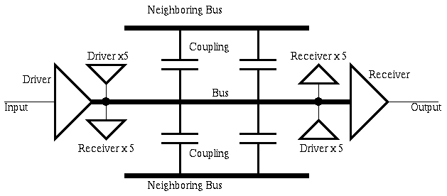
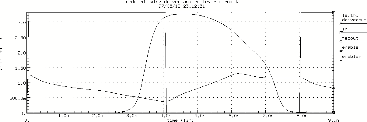
Figure 3.1. Schematic of circuit used for simulations.
In order to obtain a high level of performance from the memory section, it must be able to provide high bandwidth and low latency. Memory accesses will be pipelined to achieve high bandwidth. Since the section bus will be slow relative to the other stages of an access, the clock speed of the pipelined interface will be determined by the speed of this bus that connects the memory banks to the section controller. Traditionally, one would use a full-swing, precharged bus. Yet, such a scheme can suffer both in terms of speed and power consumption. Another concern is the noise induced on the memory banks by the bus running on top of it an switching at full-rail at more than 200MHz.
The requirements for the bus used in the crossbar are similar. The crossbar also requires a bus with minimum delay as well as low power. Because the crossbar will be placed near the memory sections, noise is also a concern.
In an effort to determine the optimal bus scheme for the above applications, four different bus schemes were evaluated. A conventional full swing bus, a precharged bus, a single-ended low swing bus [Gol94] and a differential low swing bus [Ike93] were examined. HSPICE simulations were performed to determine the performance characteristics of each scheme. Layouts of each driver and receiver were also constructed. All simulations and area estimations were performed using transistor models and design rules from the 16Mbit DRAM 0.5 um CMOS process, provided by Texas Instruments under NDA. Parasitics parameters, including resistance, wire capacitance and coupling effects, were also provided. The power supply used was 3.3 V. An interesting feature of design rules for DRAM processes is that transistors do not have the minimum possible width and length. Both are significantly increased to achieve higher yield. While the SPICE models seemed to work even with devices violating the design rules because they were smaller than minimum size, we chose to follow them in any case in order to get a more realistic comparison. The result of this decision is that in most cases, using the minimum size transistors described in the design rules would be enough to make many circuits operational and significant sizing was not necessary in many cases.
To compare these schemes, we set a speed target of a 4ns clock cycle under worst case conditions and tried to achieve that with the minimum area for drivers/receivers and minimum energy for each one. This translates to a clock frequency of 250Mhz, which is very aggressive for a 0.5um CMOS DRAM process. For an IRAM 20 mm x 20 mm chip, the worst case bus length within a section was estimated to be 8 mm. Under worst case conditions, the neighboring busses will be transitioning in the opposite direction and their coupling effects will hamper the speed at which the driver in question can charge or discharge the bus. A 50 fF load was attached to the output of each receiver. Also, each of the drivers and receivers were implemented with an enable/clock, as this functionality will be required in an actual system.
The circuit used for the HSPICE simulations is depicted in Figure 3.1. A Pi3 model was used to simulate the RC delays of the bus due to parasitic resistance and capacitance [Rab96]. Metal 2 parameters were used for the bus since metal 1 is used in the DRAM arrays and the majority of the wires in the crossbar are in metal 2. Coupling capacitance between neighboring busses was also accounted for. Finally, additional disabled drivers and receivers were attached to the bus as shown to account for any capacitive effects from the circuits.
 3.1 Bus Schemes Description
The conventional driver and receiver each consisted of a simple inverter, with the bus being driven at full swing (3.3V). The schematics, waveforms, and layout of this scheme were omitted because they are not interesting. As expected, this scheme was found to dissipate the largest amount of energy per transition, since a significantly large driver had to be used to achieve the speed goal and the bus capacitance had to be full charged/discharged
The precharged bus scheme consisted of a clocked pull-down network as a driver with a tristate inverter as a receiver. The bus is precharged to Vdd/2, which is available in all DRAM chips. The threshold of the receiver has to be placed at a point lower than Vdd/2. While precharging to Vdd/2 means that the receiver will be dissipating power during all of the evaluation phase if the wire is not pulled-down, the small size of this power consumption compared to when the bus is pulled down made this scheme attractive. The schematics, waveforms, and layout of this scheme were also omitted because they are not particularly interesting.
This precharged bus scheme was found to be faster than 4ns, even with minimum size transistors. Energy consumption is also low, due to the limited swing (0.5V). Still, it suffers from poor noise immunity and sensitivity to device variations. However, it is possible to trade off speed for larger noise margins in this scheme.
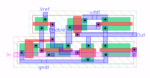
Another bus scheme that was used in this comparison was a single-ended low swing bus [Gol94]. The driver consists of an inverter controlled by a "Voltage Sense Translator" (VST). The VST basically has two states, controlled by the cross-coupled P channel transistors. The low swing output is controlled by comparing the output to a reference voltage, and uses the input to determine if the output should be higher or lower. If the output should be raised, the input voltage of the gate of the P channel pull-up is pulsed low until the output is high compared to Vref. If the output should be lowered, the gate of the N channel pull down is pulsed high until the output voltage has dropped. Through the use of feedback, the output voltage range is reduced. Notice that the input is connected through two pass transistors. This driver requires a buffer at its input to avoid corrupting the value of its input voltage and provide fast transitions.
The receiver also has two cross coupled P channel transistors, the drain of one of which is the output. The receiver brings the low swing signal to full swing, comparing the low swing input to a reference voltage and switching states based upon the result.
Using a voltage swing of 0.76 V, this scheme was found to have good noise immunity. The energy per transition is about half of that of the conventional bus scheme. Despite the complex driver, static power was found to be quite low - 1.5 nW. There are several disadvantages to using this bus scheme, however. The low swing driver was found to require 1062 um2 due to its complexity, while the receiver required 330 um2. The driver dissipates about 80% of the total energy since it has to charge/discharge the bus wire. Another disadvantage is that the input is used to charge or discharge the gates of the output transistors, which are quite large for big loads. This means that the the driver depends upon the ability of the circuit connected to the input to discharge or charge the driver's input node.
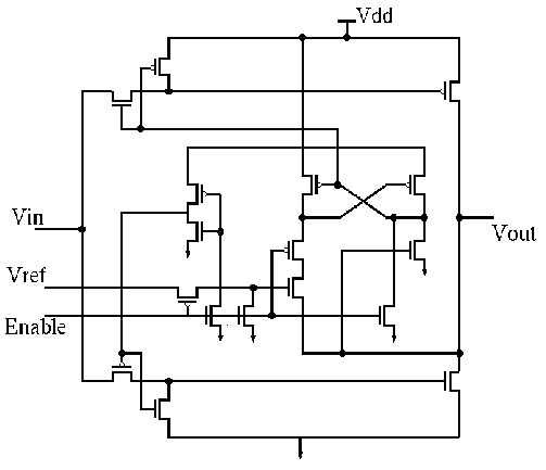
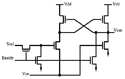
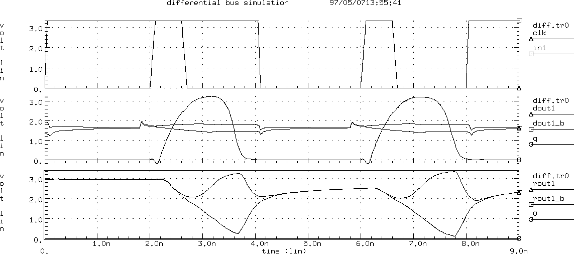
Finally, a low swing differential bus [Ike93] was also analyzed. The driver is a simple pair of minimum sized clocked inverters. Due to their limited strength, the inverters only manage to change the voltage on the wires by a small amount. The receiver consists of a source controlled sense-amplifier[Saki92]. Clock generation circuitry is also required for this scheme to shut off the driver and precharge the bus back to Vdd/2 after the sense-amplifier has reached its final state. This circuitry was included in simulations and measurements.
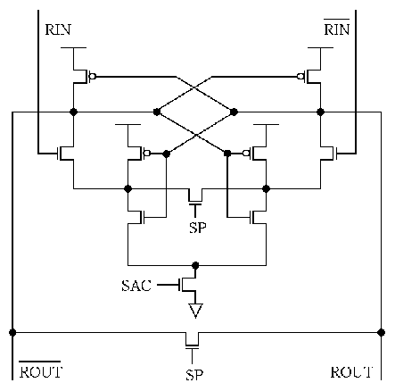
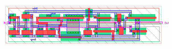
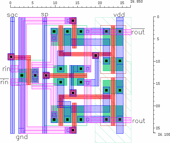
Figure 3.7 presents the schematic of the source controlled sense amplifier. This is a traditional sense amplifier augmented with a set of cross-coupled inverters used for fast feedback. These inverters also enable turning off the current path as soon as the outputs go to full-swing. The SP and SAC signals are inverses of each other. The SAC signal is raised when the sense amp is to be activated, and the SP signal is raised to reset the receiver. The differential receiver layout is depicted in figure 3.8.
 3.2 Summary of Results
| Conventional | Precharged | Low Swing Single Ended | Low Swing Differential | |
|---|---|---|---|---|
| Swing (V) | 3.3 | 0.5 | 0.76 | 0.4 |
| Average Energy/ Transition (pJ) | 13.1 | 3.93 | 7.44 | 2.06 |
| Static Power (nW) | 0.231 | 4.95 | 1.5 | 151 |
| Input Capacitance (fF) | 46 | 1.76 | 0.46/9 | 0.87 |
| Area (um2) | 337 (D) 213 (R) |
40 (D) 88 (R) |
1062 (D) 330 (R) |
342 (D) 673(R) |
| Delay (ns) | 3.79 | 1.9 | 3.91 | 0.87 |
Table 3.10 summarizes the simulation results for the four bus schemes. It is clear that if the increased area of the circuitry for the differential scheme is not an issue, it is the solution with the most advantages. In a single memory bank, since we only have to provide drivers and receivers for one full word and pitch-match them with the row buffers that contain multiple words, we don't expect this to be a problem. The precharged scheme is very sensitive to noise, so it is not a very good option for an IRAM system. The conventional driver and receiver are small, but power dissipation is large and the busses are full swing, resulting in a lot of noise for neighboring lines and underlying DRAM cells. The single-ended low swing bus scheme is also an attractive option, both for the memory sections and the crossbar. Still one would have to design it carefully to overcome its two limitations, the large driver area and the potential input node corruption at the driver.