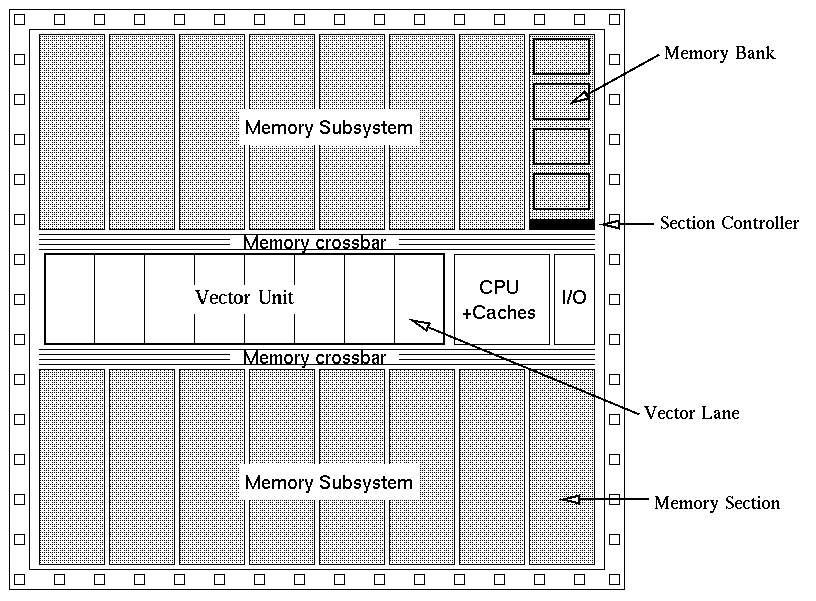
Figure 1.1. Vector IRAM system floorplan.
The integration of a general-purpose processor with DRAM memory in a single chip has been proposed to address the increasing problem of processor-memory speed gap. This idea is called Intelligent RAM (IRAM) [Pat97a]. The expected advantages of IRAM are higher memory bandwidth (up to two orders of magnitude), lower memory latency, higher energy efficiency, flexible memory granularity and board space savings. In order for IRAM to succeed, a number of problems have to be addressed in many areas, ranging from chip manufacturing to applications programming.
In this work, we study several issues about the interconnection of processor and memory within the chip, both at the architecture and circuit level. While on-chip interconnection is much more flexible than off-chip schemes, the interconnect specifications and requirements in IRAM are extremely demanding. First of all, it has to meet the processor requirements for high memory bandwidth and low memory latency in order to achieve high system performance. The ability to serve multiple independent data/address streams in parallel is also a desired feature. In the same time, it has to be area efficient (small area overhead) in order to reduce the cost and increase the area available for on-chip memory. Finally, reduced energy consumption (or high energy efficiency) is required, since the initial target for IRAM system is the embedded and portable market.
Figure 1.1 presents a potential floorplan for an IRAM chip, where the microprocessor is a RISC core augmented with a vector unit [Pat77b]. Apart from the processor, there are two other basic components: the memory subsystem and the memory crossbar. The memory subsystem is divided into blocks called memory sections. A memory section is defined as the minimum memory partition that can be potentially addressed independently and, under specific conditions, support throughput of one memory operation per clock cycle. Each section consists of a section controller and a number of memory banks. The memory crossbar connects the section controller to load/store units at the processor. Its width and flexibility determines how much of the memory bandwidth is really available to the processor and the interconnect functionality (single or multiple address streams). Still, one has to keep the size of the crossbar small. In the floorplan presented, the memory subsystem has been partitioned in two parts, with the processor in the middle, to maximize the available bandwidth. Yet, alternative layouts with the processor at one side and all the memory at the other may also be useful, either because the processor may not require high bandwidth or because we do not want to pay the potential area/energy penalty for making this bandwidth available to the processor.
To study this issue effectively, we partitioned it into two parts. The first part addresses the memory crossbar design and structure, while the second one the architecture and implementation of memory sections. The specific type of processor used in an IRAM system does not affect the results in this work. Just like the vector processor, any other valid alternative, like wide superscalar or VLIW, multithreaded processor or multiprocessor-on-a-chip, would also have multiple load/store units that communicate to the memory subsystem.
The remainder of this report is organized as follows. Section 2 presents the proposed structure and interface for the memory subsystem, specifically for the memory section. Section 3 discusses alternative structures for the memory crossbar. In section 4, we analyze the performance and characteristics of several interconnection bus schemes in a DRAM process. Finally, sections 5 and 6 present future work and conclusions respectively.