The first step when designing a high bandwidth interconnect scheme between processor and DRAM in an IRAM system is to provide the proper memory architecture and interface. DRAM architecture has been almost exactly the same for more than 15 years [Kir96]. Higher bandwidth was achieved by improvements in the interface (EDO, SDRAM, RDRAM) [Priz94]. Since the bandwidth is limited by the small number of external pins, there was no real motivation for major architectural enhancements. IRAM and embedded DRAM remove this limitation and open the way for new DRAM organizations, which can also be optimized for the specific type of logic core on the die (in this case the general processor). In this section we propose an organization for on-chip DRAM for IRAM and the corresponding interface to the processor. The main goals are high bandwidth and energy efficiency.
 2.1 Section Organization
As explained earlier, the memory subsystem in an IRAM is divided into blocks called memory sections. A memory section is defined as the minimum memory partition that can be potentially addressed independently. Therefore, multiple sections enable parallelism of accesses. Each section consists of a section controller and a number of memory banks, connected through the section bus. The controller provides the interface between the banks and the processor. Its structure and functionality is not discussed in this work, since it can depend on the specific processor architecture and it does not affect the organization of the rest of the section.
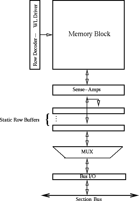
Figure 2.1 presents the block diagram of a memory bank. The basic components are the memory block, the row decoder and the sense amplifiers. Each row access delivers to the sense amplifiers a large number of bits, which are a multiple of the processor word. For simplicity. in this section we will assume that the word length is 64 bits, ignoring for the moment the fact that a single processor address may describe a larger amount of data under certain schemes. These bits can be stored in one of the static row buffers (rows of static latches). Using buffers at the outputs of the sense-amplifiers had been proposed in the past in order to decouple the next read access from reading out to the output the data of the previous one [Miy95]. Here we propose to use one or potentially more registers to provide both decoupling and caching. Multiple rows from a single bank can be concurrently open if they are stored in separate row buffers. This reduces the number of expensive RAS accesses to the memory block. The exact number of buffers is an architectural decision that depends both on performance and area overhead, but in any case there is at least one. Words stored in a row buffer can be updated or read through the section bus, one per clock cycle. In other words the section bus must be as wide as a word. There is no need for a large column decoder in the bank, since operations are either performed on a word or a whole row. We only need to be able to specify the specific row buffer or word within a row buffer involved in an operation. This information, along with the rest of the control for a memory operation, must be brought through the section bus, either in encoded or decoded form.
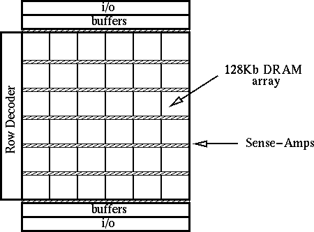
The actual floorplan of a memory bank is different from what the block diagram implies. The first reason is that it has to be constructed from the small rectangular DRAM arrays, which usually have a capacity of 128 to 256Kbits. This is the case because of the restrictions to the maximum width of bit-lines and word-lines in a DRAM array. In addition, the aspect ratio of a DRAM cell is 2:1 and the width of a sense amplifier is four times wider than a memory cell [Kir96], sense-amplifier and I/O circuits have to be placed at both sides of the memory array (folded bit line structure [Suna94]). Figure 2.2 present the floorplan of the memory bank as a two dimensional organization of 128Kbit arrays. A linear organization would fail to amortize the area cost of the decoder or the buffers and I/O circuits over a decent amount of memory. In any case, only a single memory row (word-line) is activated per access to a bank. Row buffers are placed at the top and bottom and not in between arrays to increase associativity, in other words the number of rows that can use a specific set of buffers. Transfer from internal sense-amplifiers to the buffers can be made at no cost by using segmented (or hierarchical) bit-lines [Itoh90], which would enable reductions in the number of sense-amplifier rows as well. If segmented bit lines are available, they can be constructed on top of the arrays, at the cost of an extra layer of metal.
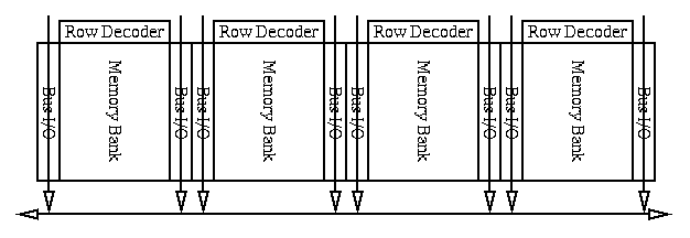
In traditional DRAM architectures, memory banks are interconnected as shown in Figure 2.3. As small number of bits (less than 8) is selected through the column decoder and driven to horizontal lines that end at the chip I/O circuit. These lines run next to the memory banks. This means that either only a few bits from those read can be transfered for processing (low bandwidth), or multiple independent banks have to be accessed to get a whole word, consuming significantly more energy.
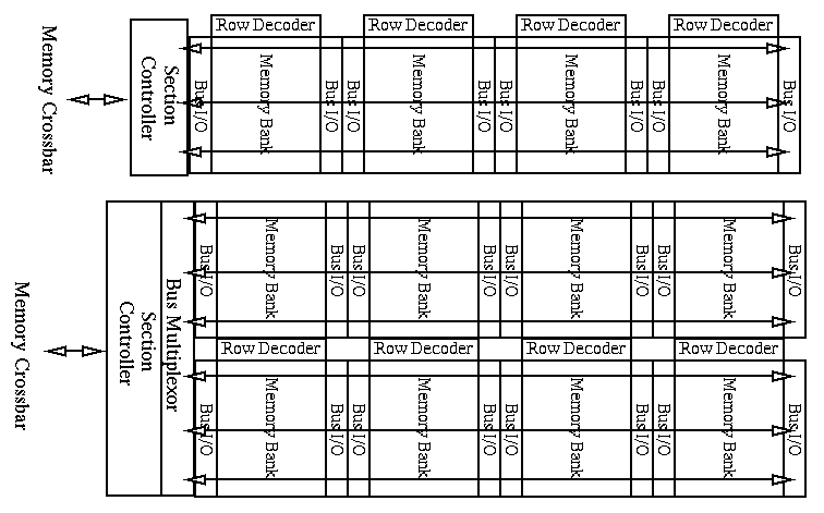
To get high bandwidth by activating a single memory bank, i.e. at low energy dissipation, we propose to interconnect banks in a memory section as shown in Figure 2.4. The section bus is routed on top of memory banks and is wide enough to transfer a whole word. Passing the bus on top of memory requires an additional layer metal. This will be available anyway, due to the requirements for building processors or high-speed interfaces in large DRAM chips. In terms of noise injected to the normal operation of the array, this can be reduced by using low-swing busses or having supply distribution laid out between memory and the bus wires [ISSCC97]. In addition, it has been demonstrated already that this is feasible [Suna95]. We analyze appropriate schemes for the section bus in section 3.
Depending on the exact size of the bank, the number of sections desired and the size of the memory subsystem, we can organize the bank in a section either in single or multiple rows. Multiple rows enable the elimination of some decoders, but need some glue logic to implement the multiplexing/demultiplexing of the multiple busses into one. Since all these busses are logically one and, therefore, only one can be active per clock cycle, this should be simple to implement.
2.2 Design ParametersThe above described memory architecture has a number of design parameters that can be adjusted according to the requirements of a specific implementation. Here, we will try to define the implications of each parameter to area, potential performance and energy.
The first design parameter is the number of memory sections. As described earlier, the number of memory sections determines the available access parallelism. While this number has no effect on memory size, it can increase significantly the area of the memory crossbar, if we decide to address each one independently. The increased number of sections also puts high demands on the address generation unit on the processor side as well, due to TLB lookups, conflict resolution etc.
Given the desired number of sections and the total area for memory, the next design parameter is the size of a memory bank. Larger bank sizes are attractive since the area cost of bank periphery is amortized over a large memory area and there are less receivers/drivers on the section bus. Specifically, increased bank height amortizes the cost of row buffers and I/O circuits, while increase bank length amortizes the cost of the decoder. On the other hand, in terms of energy it is better to have many small banks. On each RAS access, we need to activate a whole bank, thus the smaller the better. The width of the bank has a second effect as well. By increasing it, we also increase the width of row buffers, in other words the "block size" of our cache. While initially increasing the block size is good in terms of performance due to prefetching, after a certain point we end up prefetching data that will never be used, which is unacceptable in terms of energy.
A final parameter is the number of row buffers per bank. Obviously, increasing the number of buffers comes with an area penalty both due to the area they take up and the additional complexity of multiplexing at the bank's interface. Additional cache size does improve performance (up to the point where compulsory misses dominate), but it may not be worth it to sacrifice much of area for it, as it could be used for on-chip DRAM.
2.3 Area ConsiderationsTo quantify the area requirements and tradeoffs of our architecture we used the published results for a 256Mbit DRAM 0.25um CMOS technology by NEC [Taka96]. In this technology the basic DRAM array has a capacity of 128Mbit.
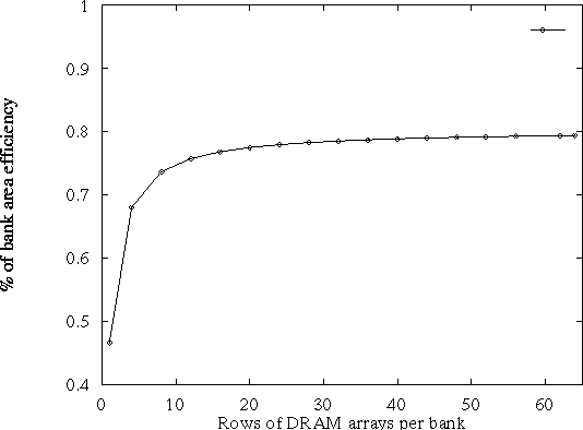
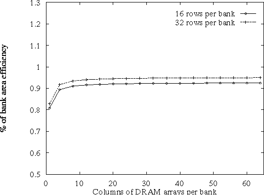
The first thing we examined is how many rows of arrays are necessary per bank in order to amortize the cost of the I/O periphery (SAs, row buffers, bus I/O circuits). Figure 2.5 presents the percentage of area utilization for a bank (area of DRAM cells/bank area) as a function of the numbers of rows of DRAM arrays. In this case a single row buffer and a single column of arrays is assumed. Eight rows of DRAM arrays are enough to fully amortize the area cost of the periphery. A similar analysis was performed to find out the number of DRAM array columns necessary to amortize the area cost of the decoder. This is presented in Figure 2.6. The area cost of the decoder is fully amortized with 4 columns.
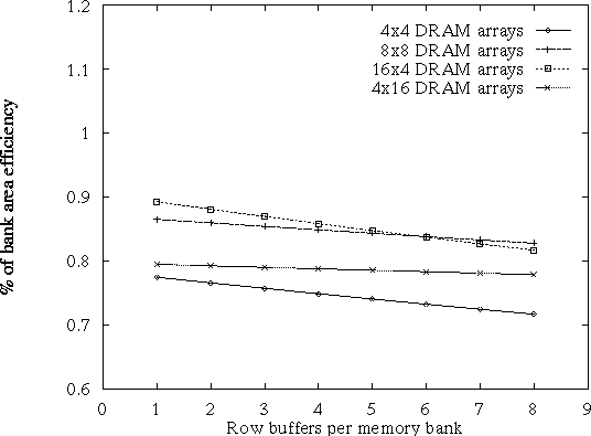
Another issue we analyzed is the area penalty for adding more than one static row buffer. Figure 2.7 presents the percentage of bank area efficiency as a function of the number static row buffers, for a few possible combinations of rows and columns. In any case the area penalty does not increase more than 10%. For a small number of buffers (2 or 4) it is less than 2%. This implies that the area cost of adding caching to the DRAM architecture is insignificant. Of course, the performance benefits from using this form of caches and the exact number of buffers necessary still need to be quantified. Table 2.8, presents the number of cache bits per Kbit of DRAM for our architecture for various bank sizes and number of rows. For comparison, a current high-end workstation has .5 to 4 L2 cache bits per Kbit of DRAM.
| Number of row buffers per bank | ||||
|---|---|---|---|---|
| 1 | 2 | 4 | 8 | |
| 2Mbit (4x4) | 0.5 | 1 | 2 | 3 |
| 4Mbit (4x8) | 0.5 | 1 | 2 | 3 |
| 8Mbit (8x8) | 0.25 | 0.5 | 1 | 2 |
| 16Mbit (16x8) | 0.125 | 0.25 | .5 | 1 |
Finally, another concern about the bank size is how many banks fit in a chip. Table 2.9 presents the number of banks that can fit in a 20mm x 20mm chip, where three quarters of the memory are dedicated to the memory subsystem. In all cases the number of static buffers per bank is 4. Increasing the bank size naturally decreases the number of banks that can fit on-chip. We can also see that with 4 columns and 4 rows of 128Kbit DRAM arrays per bank, a large number of banks can fit on chip. Thus, one can potentially built a large number of memory sections. For example, for the 4x4 bank organization, one can built 32 sections with 6 banks each, or 16 sections with 12 banks each etc. While the number of sections may be determined by the complexity of the crossbar and the circuitry that generates addresses for these independent address streams, a large number of banks is still desirable from an energy perspective, as explained earlier.
| Rows of 128Kbit Arrays per Bank |
Columns of 128Kbit Arrays per Bank | |||
|---|---|---|---|---|
| _ | 1 | 4 | 8 | 16 |
| 4 | 648 | 194 | 100 | 51 |
| 8 | 350 | 106 | 55 | 28 |
| 16 | 182 | 55 | 28 | 14 |
2.4 InterfaceHaving defined the bank architecture and potential organizations of memory sections, we also need to define the memory interface. This includes the commands that each memory bank can understand and the way they are executed. The main concerns of the interface design are to define a flexible set of commands that will enable both high bandwidth and energy efficiency, without imposing large memory access delays.
To define the appropriate interface, we examined the architectures and corresponding interfaces of several high-performance DRAMs [Prin96][Ohsh94]. An interface similar to that of RDRAM [Kush93] was not preferred since most of architectural decisions associated with it were based on characteristics of off-chip interconnect. RDRAM uses narrow busses and achieves high-bandwidth at the cost of higher latency. Still, in our architecture the section bus is significantly wider, so high-bandwidth can be achieved without hurting latency. In addition, the packet-based interface used in RDRAM would add extra latency and complexity without offering any advantages. For these reasons, our interface was based on interfaces defined for Synchronous DRAM.
Several variations for SDRAM interfaces exist. The basic approaches are the pipelined interface [Tak94], the prefetched interface [Choi94] and the combined pipelined and prefetched interface [Suna95]. In our architecture, prefetching is performed by reading memory rows to row buffers. Apart from the word actually addressed, a few more words will be prefetched to the row buffers. Further prefetching, to the section controller for example, would probably be energy wasteful, unless activated only when necessary. For this reason we decided not to provide further prefetching in an implicit fashion. If it is needed, it can be explicitly implemented through read commands.
| Command | Arguments | Operation |
| Precharge | #bank | Precharge bit-lines |
| Read2B | #bank,#address,#buffer | Read memory row to buffer |
| Write2B | #bank,#address,#buffer | Write back buffer to memory row |
| Read2S | #bank,#buffer,#word | Read word from buffer to section bus |
| Write2S | #bank,#buffer,#word | Write word from section bus to buffer |
| Refresh | #bank,#row | Refresh memory row |
Table 2.10 presents the commands of the proposed interface for the IRAM memory architecture. These six commands are transfered to memory banks through the section bus. Read and write RAS accesses just transfer rows (multiple words) from memory rows to a row buffer and vice versa. Read accesses have optional restoring. Restoring memory data that will be overwritten soon is energy-inefficient. From the energy perspective it is better to make all the updates on a specific row in a row buffer and write it back only once at the end. Commands Read2S and Write2S transfer one of the words in the data buffer to the section bus and vice versa. Refresh goes does not go through the row buffers in order to avoid thrashing the contents of the cache. This is the main reason that we do not use the sense-amplifiers as cache as proposed in many systems [SPN96]. In addition, we chose to provide a refresh-row instead of a refresh-bank command, to provide the flexibility for the operating system to refresh only the memory pages actually used by applications. This can reduce the energy cost of refreshing.
| Command | Stages |
| Precharge | Precharge bit-lines |
| Read2B | Row decoder |
| RAS access and amplification | |
| Row buffer Latch - (*) restore row | |
| Write2B | Row decoder - Load SAs from buffer |
| RAS access | |
| Read2S | Word selection/multiplexing |
| Drive section bus | |
| Write2S | Drive section bus |
| Latch word to proper buffer | |
| Refresh | Row decoder |
| RAS access and amplification | |
| Restore row |
The execution of each of these commands can be broken into discrete stages and, therefore, pipelined. Table 2.11 presents the basic steps for each command. In an actual design, the slowest of these stages will determine the clock cycle period of the synchronous interface. From there on, one can pack as many of the remaining stages as possible in a single clock cycle. The common case in current SDRAM is that the transfer over the bus that connects banks to external I/O circuitry (section bus in our case) is the longest step. For this reason we examine the performance of several bus schemes and techniques (speed, power, area and noise) in the following section.
One should notice that memory banks do not need to know who generated the commands. In other words, this interface decouples the design of the memory system from the design and functionality details of the section controllers and the load/store units. These commands may be directly generated by load/store units or by the section controllers, after decoding some other type of commands issued by the processor. The exact place of command generation depends on where we want to add the complexity and the overhead of address checks, cache tag comparisons etc. Thus the same bank design can be used with multiple significantly different IRAM processors. It also allows the design of the memory system to proceed before the processor architecture has frozen.