Clock Control
Introduction
The clock control logic brings a link into a locked state so that
data transmission can occur. When the system first starts up, there is
no lock between the transmitting serial link and the receiving serial
link. Each transceiver continuously sends K28.5, the control character
signifying the sender is not locked, while processing the incoming
samples to first obtain bit lock and then obtain byte lock by
searching for K28.5 or K28.1. As soon as a receiver is byte locked it
begins to transmit K28.1, the locked pattern. When both transceivers
are byte locked, both are transmitting and receiving the locked
character. Each transceiver is locked and both know the other is
locked. The system is now ready for data tranmission.
Clock Control Operation
There are several steps in bringing the system into a locked state
for data transmission. First, the DLL must lock so that the clock
outputs are equally spaced. Then, bit lock is required so that the
sampled data is valid. Finally, byte lock is required to define the
boundary between data characters. The clock control circuitry ensures
that the serial link is both byte locked and bit locked. The byte lock
circuitry is activated at startup or when the serial link loses
lock. The bit lock circuitry is constantly active in agreement with
the tracking scheme.
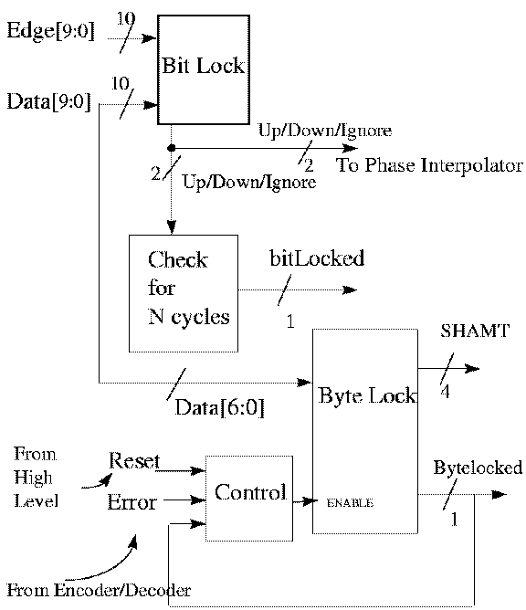
Figure 2.4.1 - Clock Control Diagram
- At startup, before the clock control begins to
function,the DLL must first lock.
- 10 data samples and 10 edge samples are input to the clock
control for bit lock. Judging from the transitions in the samples,
the bit lock block determines whether the sampling clock is early or
late with respect to the data eye and outputs a 2-bit up/down/ignore
signal to the phase interpolator to adjust the sampling point
accordingly. Bit lock is achieved when the 2-bit output to the phase
interpolator alternates between 'up' and 'down'. This pattern of the
output must continue for a number of cycles before the serial link is
considered bit locked. The exact number of cycles needs to be
determined from simulation once the entire serial link is integrated.
Data samples do not represent valid data until the serial link is bit
locked.
- The byte lock block compares input data with K28.5 and K28.1 to
determine the offset of the beginning of the current byte frame. This
offset is output as 'SHAMT' to the data shifter, which in turn shifts
the data byte to the correct position. The serial link is then byte
locked and ready to transmit and receive, and the byte lock circuit is
disabled. The serial link could potentially lose byte lock over time.
This would either be detected by the encoder/decoder unit when invalid
data is decoded, or from a higher level. Both cases would activate the
byte lock circuitry again to obtain byte lock.
Bit Lock
A transition consists of an edge sample and its two neighboring (and
different) data samples. If the edge agrees with its preceding data
bit, then the sampling point is 'early', otherwise, it's 'late'. For
every 20-bit input to the bit lock block, all the transitions vote and
majority rule applies to reach a decision and adjust the sampling
point through the phase interpolator. If there are an equal number of
early's and late's, then 'ignore' is output.
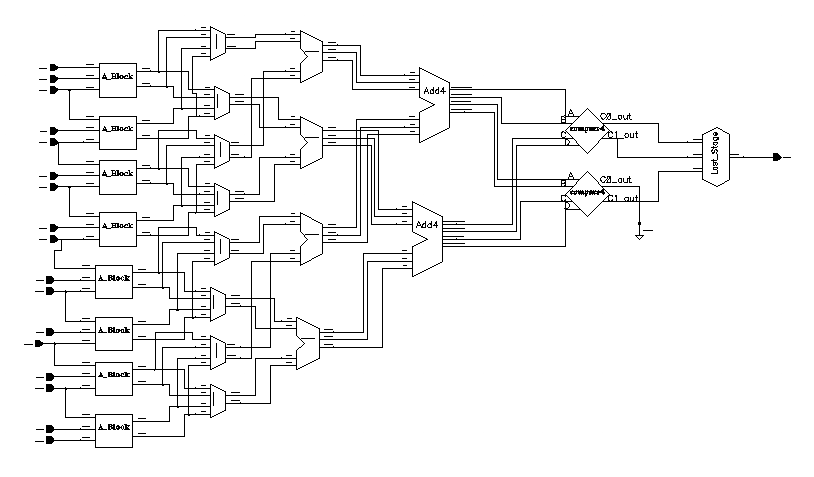
Figure 2.4.2 - Bit Lock Schematic
A schematic of the bit lock implementation is shown in figure
2.4.2. 10 data samples and 10 edge samples form a maximum of 9
possible transitions. Only 8 of these transitions are used the
majority-vote logic to reduce hardware, and are represented by the 16
inputs on the right. The number of 'earlys' and the number of 'lates'
are summed and then compared to generate the output. CMOS static
logic is used to implement the circuit. Total area is
32000um2, power is 3mW, and delay is 4 ns.
Byte Lock
When the byte lock circuit is active, the incoming data is either
K28.5 or K28.1. The byte lock block compares the input data byte,
which is a shifted version of K28.5 or K28.1, with both K28.5 and
K28.1. The output is the offset needed to shift into the correct byte
frame position.
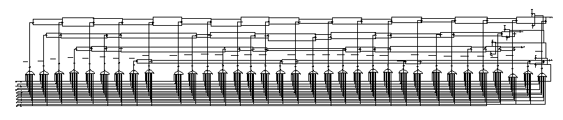
Figure 2.4.3 - Byte Lock Schematic
The first circuit scheme considered was the brute force method of
comparing the input with every possible shifted version of K28.5 and
K28.1. But the amount of hardware required makes this scheme not
feasible. To save hardware, another scheme was considered in which a
shifter shifts the input bits through all possible combinations to
perform the comparisons. This scheme was attractive in that the
comparison hardware is not replicated for every possible pattern. The
disadvantage is the timing. In fact, to avoid wrap around of bits,
there are a total of 40 possible shifted versions of the input and
thus 40 clock cycles are needed to obtain byte lock in the worst
case.
The current scheme takes an entirely different approach from the
previous two. It was noted that of the 20 bits of the input, the first
7 bits are distinct for every shift position and those alone are
enough to decode the 4-bit output shift offset. And it turns out that
only 34 of the 40 possible patterns are distinct. The circuit was
layed out like a PLA, with a 7-input AND plane and a 34-input OR
plane. Dynamic logic was used to reduce area considerably. The 10ns
clock period is long enough to accomodate both the precharge of the
circuit and the propagation delay of the 7-input NAND gates. The
34-input OR gates do not impact performance since all 34 NFET's are in
parallel. This scheme not only ensures byte lock within 1 clock
cycle, it also does so within reasonable area. The total area is
32400um2, 7ns delay (with 5ns precharge) and negligible
power.