Clock Phase Generation
The bit time for a 1 GHz link is 1 ns, and for a tracking scheme two
samples are are needed per bit time. To achieve this, the desired
output from the clock phase generation block is 20 equally spaced
phases of a 10ns clock period. The delay between each phase should be
500 ps. Either a delay locked loop (DLL) or a phase locked loop (PLL)
could be used to generate the these phases of the system clock. PLL's
generate their own clock by using a ring oscillator whose frequency of
oscillation is adjusted to match a given input clock. DLL's do not
have the capability to oscillate at a range of frequencies, but
instead precisely delay the travel of clock transitions down a line of
delay elements. The delay is controlled by circuitry which compares
the input clock with the output of the delay line and adjusts the
delay of the delay elements until they match, meaning the total delay
of the delay line is one clock period.
A PLL has the advantage of being programmable and is well suited to
frequency multiplication. Also, PLLs do not pass any jitter from the
reference clock to the output clock since PLL's generate their own
clock. The clock signal generated by a PLL does, of course, have a
certain amount of inherent jitter. The feedback loop used to adjust a
PLL's frequency of oscillation has the possibility of becoming
unstable since it is a second order system. This places a stringent
stability requirement on the loop gain and complicates the design and
implementation of the PLL.
A DLL has the advantage of being relatively simple to design as it is
only a first order system and therefore has no stability
requirements. DLL's pass any jitter from the input clock to the
output, however, and can have false locking problems. This occurs when
the DLL has locked to two or more periods of the input clock, and must
be avoided.
For this project, no frequency multiplication is required since a high
frequency crystal oscillator will be present on the PCB. Because this
signal will be coming from a crystal oscillator, the input clock will
be very clean and will have very little noticable jitter. For these
reasons, a DLL was selected for the clock phase generation. It is
simpler to implement and meets our requirements. A block diagram of a
DLL is shown in figure 2.1.1. The basic components of a DLL are the delay
elements, a phase detector (or phase frequency detector), a charge
pump, and a loop filter. A PLL shares the same components, but the
components are connected in a different fashion and the loop filter is
more complex than a simple capacitor.
To handle the false locking problem, whenever the link is reset, the
DLL will be reset to minimum delay. When the DLL attempts to lock, it
will increase the delay of the delay line until precisely one period
of delay exists in the line, avoiding the false locking problem. A
design decision also exists in choosing a phase detector or a
phase-frequency detector. This issue is discussed in that section.
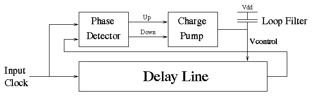
Figure 2.1.1 - Delay Locked Loop
The number of delay elements used in the DLL would be 20 if the DLL
was locked to one full period of the input clock (10 ns). In this
mode, the input and the output of the DLL would be exactly in phase
when the DLL is locked. However, the more delay elements there are in
the delay line, the more jitter there will be at the output, since the
jitter introduced by each delay element accumulates as the signal
travels down the delay line. With 20 delay elements, simulation
results revealed inherent jitter of just the delay line with biasing
in the 100 ps range, caused by capacitive parasitic coupling of the
delay elements through the bias nodes. This jitter is not acceptable,
especially in simulation results. Since the delay elements are
differential to provide excellent noise rejection, an alternative is
to lock the DLL to half of the input clock period, forcing the
positive input clock to be exactly in phase with the negative output.
This results in a 10 element delay line which has much less inherent
jitter, closer to 10-20 ps.
Using a shorter delay line now requires the use of both the positive
and negative outputs of the DLL to be used for clocking. This means
that the input clock must have a precisely controlled 50% duty cycle
to ensure proper spacing between DLL outputs. Since the off chip
crystal oscillator that will provide the input clock to the DLL will
not have a 50% duty cycle (they commonly do not), we will have to use
a crystal osciallator that will have twice the frequency we desire and
will divide the clock by two on the way into the DLL. For this reason,
we are planning to use a 200 MHz crystal oscillator and divide its
frequency down to 100MHz with 50% duty cycle.
Delay Element
A delay element provides a way for the delay through the stage to be
controlled, usually by a voltage. A current starved inverter is one
way a delay element might be implemented, but the delay through a
simple inverter fluctuates with the supply voltage and has very poor
noise rejection. A differential scheme provides much higher noise
immunity and is shown below in Figure 2.1.2 [Man96, Hor93]. The
current through the differential delay element is controlled by Vbn
and is dynamically biased to compensate for drain and substrate
voltage variations, so a cascoded current source is not necessary.
This current controls the delay through the delay element. To provide
supply noise rejection, symmetric loads are used to generate an I-V
characteristic similar to that of a resistive, linear load [Man96]. In
order to maintain the linearity of the loads as the current flowing
through them changes (and hence the delay), the swing of the delay
element is allowed to vary with the load bias Vbp.

Figure 2.1.2 - Schematic of Delay Element
Replica Bias
The bias voltages Vbp and Vbn are generated by a
replica bias unit which is made to be fast enough to track high
frequency supply noise and substrate noise. Supply noise is
anticipated to be a dominant noise source for this link when placed on
an IRAM chip, even with separate supply and ground pins. With replica
biasing, the delay of a delay element will not vary with operating
conditions or process variations.
Logically, the replica bias unit consists of a half buffer replica of
the delay element and a transconductance amplifier. A diagram is shown
in figure 2.1.3. The low value of the output swing, Vbp, is set to be
equal to the control voltage Vctrl by adjusting the amount of current
through the half buffer replica. This current is controlled by Vbn. If
the amplifier is designed to have a wide bandwidth, Vbp and Vbn will
be adjusted dynamically as the supply and ground voltages vary, even
at high frequencies.

Figure 2.1.3 - Replica Bias Logical Diagram
A schematic of the replica bias unit is shown in figure 2.1.4. The
amplifer has inputs Vctrl and Vbp. It adjusts the current through the
half buffer replica until they are equal. An additional buffer stage
is also necessary to decouple the replica bias amplifier input from
the actual Vbp seen by the delay elements, but it is not shown here
for clarity. A startup circuit which pulls a minimum amount of current
through the amplifier when Vbn is zero volts, also not shown, is
required to force the amplifier to turn on.

Figure 2.1.4 - Replica Bias Schematic
The frequency response of the replica bias unit is shown in figure
2.1.5. Vdd was used as the AC source for these simulations. The plot
shows that Vbp tracks exactly with Vdd out to about 100 MHz. Past this
frequency, deviations are still small but will affect jitter. Noise on
Vdd that has frequency components higher than 100MHz will adversely
affect the delay of the delay elements because the bias unit can not
keep up with supply fluctuations at that rate. Vbn should be resistant
to changes in Vdd as well, and it also tracks well out to about
100MHz. Supply noise with strong frequency components in the
100-200MHz range is expected from a nearby processor, so rejection of
noise at these frequencies is expected to be an important issue for
reliable performance.

Figure 2.1.5 - Worst Case Replica Bias
Frequency Response
In order to make the amplifier very fast and allow it to have a wide
frequency range, multiple half buffer replica stages are actually
used, connected in parallel. This allows much more current to flow
through the feedback path of this bias unit and allows it to respond
to changes faster. The tradeoff is, of course, additional power
dissipation. Through experimentation is was found that the benefits of
adding parallel stages started to decrease past six stages.
Phase Detector
The phase detector used in this project is the edge-sensitive, 180
degree locking detector and is shown in Figure 2.1.6 [Sid97]. When the
input clocks have identical duty cycle, there will be a 180 degree
phase difference between the falling edges of the inputs. Compared
with a conventional phase frequency detector, this design doesn't have
any state, so false locking due to glitching is avoided.

Figure 2.1.6 - Phase Detector Schematic
The disadvantage of this phase detector is that current is always
charging or discharging the output of the charge pump, so a small
current must be used in the charge pump to reduce jitter. Since a
small current is used in the charge pump, lock time is increased.
Charge Pump
There are many different ways to implement a charge pump. The design
of this circuit is important because it must be constructed in a way
that will keep it from causing any unwanted fluctuations in the
control voltage. To accomplish this, an important aspect of the charge
pump is that the paths from control to output for both the pull up and
pull down paths should be symmetric. That is, when the up signal is
active, the amount of time it takes for the current to charge the
output node should be the same as the amount of time it takes for an
active down signal to pull current out of the output node. Some charge
pumps in the literature, such as that shown in [Man96], do not meet
this requirement.
For this project, we decided to use two differential pairs to switch
current to the output or from the output. A pmos differential pair is
used to control the current into the output node, and an nmos
differential pair is used to control current from the output node. The
schematic is shown in figure 2.1.7. One of the differntial pair inputs
is connected to a reference voltage, and if the inputs are above or
below this reference, current will be sent through the appropriate
device.
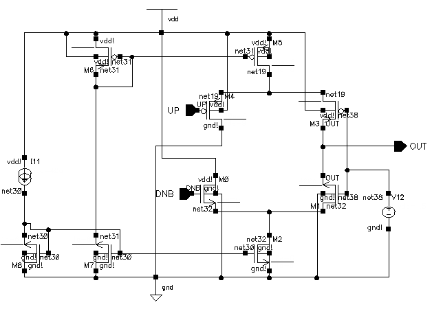
Figure 2.1.7 - Charge Pump Schematic
One complication with this charge pump is that it now requires up and
down signal inputs that are not full swing, which is what the phase
detector has as output. Thus the swing of the up and down signals must
be converted to the appropriate smaller swing. This is accomplished by
the following "swing reducer" circuit shown in figure 2.1.8 which
basically consists of a source follower and two diodes to limit the
minimum voltage at the output.

Figure 2.1.8 - Swing Reducer Schematic
Area and Power Results
Layout has been completed for some of the components. The area and
power results are summarized in the following table for both the
receive DLL and the transmit DLL. Area for the replica bias unit is an
estimate. The two DLL's only differ in thier loads. The transmit DLL
generates clocks for the serializer, which requires full swing input
clocks. The receive DLL generates clocks for the sampling unit, which
requires small swing, but level shifted input clocks.
| 10 Element Receive DLL |
10 Element Transmit DLL |
|---|
| Part | Static
Current | Size |
Number | Power | Area |
Number | Power | Area |
|---|
| Delay Elements | 100uA | 10um x 40um |
10+4 | 4.62mW | 5600um2 |
10+4 | 4.62mW | 5600um2 |
| Replica Bias | 1.6mA | 12880um2 |
1 | 6.6mW | 12880um2 |
1 | 6.6mW | 12880um2 |
| Charge Pump | 120uA | 1496um2 |
1 | 396uW | 1496um2 |
1 | 396uW | 1496um2 |
| Phase Detector | 0 | 1078um2 |
1 | negligible | 1078um2 |
1 | negligible | 1078um2 |
| Full Swing Buffer | 40uA | 9um x 15um |
0 | - | - |
20+8 | 3.7mW | 3780um2 |
| Level Shifter | 50uA | 250um2 |
20+8 | 4.62mW | 250um2 |
0 | - | - |
| Total | | | |
16.2mW | 21304um2 | |
15.3mW | 24834um2 |