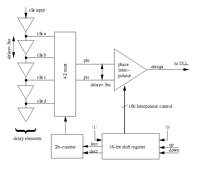
Figure 2.2.1 - Phase Interpolator Block Diagram
The phase interpolator is a critical circuit in the receiver of the serial link. It allows the receiver to adjust the phase of its sampling clocks in very fine increments.We chose to implement a current-controlled phase interpolator, as described in [Sid97] rather than a voltage-controlled interpolator, as described in [Enam92]. The voltage controlled interpolators were much less linear and more difficult to control, since they required analog control inputs. Although the current-controlled interpolator was bigger and consumed more power its outputs were much more linear and it took digital inputs.
Figure 2.2.1 shows a block diagram of the interpolator. Four equally spaced clocks are generated and fed into a 4:2 multiplexer. The two bit counter selects which of the two clocks to interpolate between, and the weight of the two input clocks on the output is determined by the 16 bit shift register.
The delay elements are identical to the delay elements of the DLL and are biased off the same references, so that their delays will be the same. For 1 GHz link speed, the delay elements of the receive DLL will be spaced by 0.5 ns in order to sample both data and edges. Therefore, the four inputs to the phase interpolator will be spaced by a total of 1.5 ns. Since the data eye is only 1 ns wide, the range of the phase interpolator is 0.5 ns larger than necessary. This is important because the delay elements in the DLL and the interpolator may not be precisely matched since their loads may differ slightly. If we only used three inputs to the interpolator, spaced a total of 1.0 ns apart, and the delay turned out to be slightly less than 1 ns, there is the possibility that the center of the data eye would fall outside of the interpolator's range. By using a larger than necessary range, we can guarantee that the center of at least one data eye will fall within the range of the interpolator.
The phase interpolator has a granularity of 16 steps per clock phase, so that there are a total of 64 phase steps, each spaced by 31.25 ps. We could have just interpolated between the first and last clock edges, spaced 1.5 ns apart, but instead chose to always interpolate between adjacent edges, spaced 0.5 ns apart. This is because the interpolator is not very linear, and by interpolating between smaller equally spaced steps we impose some linearity.
The weight of the phase interpolator is controlled by a 16-bit shift register. We could have also chosen to use a 4-bit up down counter, where each bit had twice the weight of the previous bit, but chose the shift register since it was simpler to implement and simpler to complement, since we also needed the complement of the 16-bit weight. The area and power of the shift register were both insignificant (37,500 um2 and 53 uW).
The inputs to the shift register are the up and down signals produced by the bit lock logic. The shift register shifts 1's in on the left and 0's in on the right. Control logic senses when the shift register contains all 1's or all 0's. This logic will then increment or decrement the 2b counter appropriately, which will shift the two edges being interpolated between. The shift register will then continue shifting in the opposite direction.
We examined two types of current-controlled phase interpolators, type-I and type-II, as described in [Sid97]. Type-I places the control switch below the clock inputs, so that the clock inputs can be shared among all 16 diff pairs. Although this would be a smaller design, it is less linear than the type-II that we chose to implement. The reason is that one side cannot be entirely shut off with the type-I interpolator. Even if all of the current is through the phi branch, the psi inputs will still effect the output due to coupling from the gate to drain of the diff pair inputs.

Figure 2.2.2 shows a schematic of the type-II interpolator we chose to implement. Its clock inputs are separated from outputs by control switches, to avoid coupling to the output through Cgd. The nmos current sources supply 1/16 of total current, and use the same biases as the receive DLL.
The nmos part of the block shown above is repeated 16 times, so that there are 16 phi diff pairs and 16 psi diff pairs. The total current through the interpolator is constant and will be divided among phi and psi diff pairs based on the digital interpolator weight, which shuts off or turns on the appropriate number of phi and psi pairs through the complementary ctl[i] and ctlb[i] inputs. Depending on the current through phi and psi, the phase of omega will shift between the two.
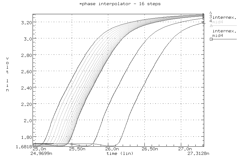
Figure 2.2.3 shows the outputs of the phase interpolator. The hspice simulations are from the extracted layout. The dark lines are the four equally spaced outputs of the delay elements, and represent the phi and psi inputs to the interpolator. The light grey lines are the 16 phase steps between the first two clock edges. Although the edges are not perfectly linear, the largest step of 70 ps is only 39 ps greater than the nominal phase step. The smallest step is 1 ps.
When in lock, the phase interpolator will bounce back and forth between two adjacent steps. Therefore, the largest phase step determines the maximum peak-to-peak jitter of the receive DLL outputs. We considered using 8 steps instead of 16, but the maximum phase step was 145 ps, which would have led to unacceptable peak-to-peak jitter. Using more than 16 phase steps is difficult since all the gates of all phi and psi inputs must be driven by the same delay element. In order to have 16 steps, these gates were made small, but it would be difficult to make them much smaller and still have acceptable transconductances.
The control logic controls both the weight of the interpolator, through ictl[15:0], and the two clock edges that are input to the interpolator, through sela-seld. A schematic of the control logic is shown in figure 2.2.4. The logic on the top left translates the up/down pulses from the bit-lock logic into left and right signals for the shift register. It bases this decision on the state held by the 2-bit counter, which keeps track of which two clocks are being interpolated between. The outputs of the 2-bit counter feed the logic on the bottom right to select the correct muxes.

It is important to think about what may happen when the phase interpolator is at the edge of its range. It would be bad to have the interpolator wrap around while in lock because it would either lose a bit or sample a bit twice. But it may also be bad to force it to freeze once it reaches the edge of the range if the eye is outside of this range. What we would like to do is allow it to wrap around during acquisition when we do not care if we lose a few bits. We could leave some padding on both ends of the range that it can only go into once it is in lock, allowing a certain amount of phase drift once in lock.
The shift register controls the weight of the interpolator phase by shifting ones and zeros back and forth. Ones are shifted in on the top left and zeros are shifted in on the bottom right. Control logic detects when the shift register is full of ones or zeros and will toggle the relationship between early and late and shift left and shift right.
Need more description or picture??
The table gives a summary of the power and area numbers for the different parts of the interpolator. The interpolator input drivers are four delay elements and four buffers, and may actually be a part of the transmit DLL, so that they will not actually consume additional power. The rest of the circuits have insignicant area and power when compared to the rest of the circuit. The control logic area is estimated based on the number of gates and flip flops and the size of the gates and flip flops that have already been laid out.
|
Part |
Size |
Number |
Total Area |
Total Power |
|
Interpolator |
9 um x 16 um |
32 |
4500 um2 |
920 uW |
|
Interpolator Input |
10 um x 40 um |
5 |
2000 um2 |
4.6 mW |
|
16b Shift Register |
250 um x 150 um |
1 |
37500 um2 |
53 uW |
|
Rest of control logic |
~100 um x 150 um |
1 |
15000 um2 |
small |
|
Total |
- |
- |
57000 um2 |
5.6 mW |