Serializer
The serializer takes as input the 10 bit data from the encoder and
multiplexes this data onto the outputs by logically ANDing the
appropriate clocks from the transmit DLL [Lee95]. The input data and their
complements are required to produce the differential outputs. The
transistors are sized to provide the appropriate swing to the transmit
circuitry. The output swing is from approximately 2V to
Vdd. The entire circuit of the serializer in figure 2.5.1 is not shown.
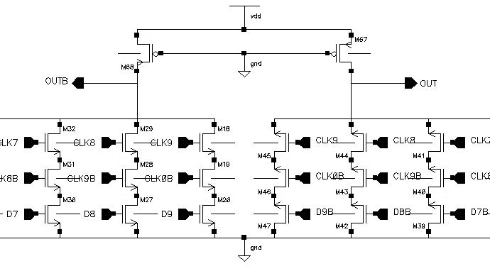
Figure 2.5.1 - Schematic of Serializer
When clock8 and clock9B are both high, D8 and D8B will be placed on
the output for that 1 ns. When clock 9 and clock0B are both high, D9
and D9B are placed on the output for the following 1ns, and so on.
The last inputs to the serializer may not be held long enough to
ensure that the data will properly be serialized. The flip-flops which
hold the data for the serializer must refresh to the next data values,
severly limiting the setup and hold times of the last data bits on the
serializer. The additional flip flops in figure 2.5.2 are used to fix this
problem.
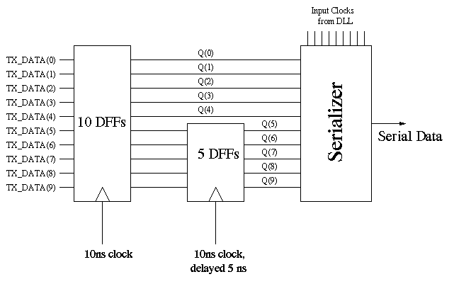
Figure 2.5.2 - Block Diagram of
Serializer Interface
Power and area of
this design are summarized at the end of this report.